
| Industry | Usage | Applied Product |
|---|---|---|
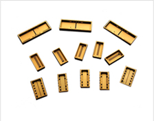
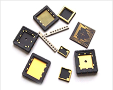
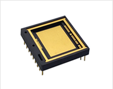
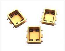
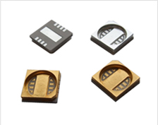
| Package | Crystal/Oscillator/SAW packages, Ceramic/Metal package, Hybrid packages, Optical Package, Power dissipation package, Sensor packages, LED packages, Monolithic microwave hybrid technology | |
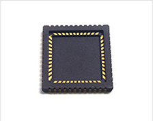
| IT and Electronics | HTCC | Amp housing, Custom pin grid array(PGA), High Frequency Feedthroughs, Leadless chip carriers(CLCC), Multichip module(MCM), Pad array carriers(BGA), Quad Flat packs(QFP), Quad No lead(QFN) |
| Optoelectronics | CMOS, CCD, CLCC, Infrared, ultraviolet image sensor | |
| Resistance | Curler, soldering iron, PTC, bidet and plasma reactor | |
| Vehicle | Electric Part | Power electronics PCB, LED lamp, honeycomb, PTC heater, ion generator, glow plug, etc. |
| Semiconductor | Equipment | Probe Card, ESC, susceptor, boat, tube, chuck, etc. |
| Bio | Human Body | Body material, artificial material and dental parts |
Current R&D area is the insulating ceramic package which mainly uses HTCC (high temperature co-fired ceramic) and Al2O3 (alumina), of which internal electrode uses the metal with high melting point such as W, Mo or Mn for internal layer wiring and inter-layer conduction, and which is sintered at 1,500℃ or higher under reduction atmosphere with hydrogen, nitrogen or both, to meet required mechanical and electric characteristics.
As the semiconductor, mobile communication and LED markets have recently expanded significantly, the trend is wide growth of applications required of high temperature property, high chemical resistance, high thermal conductivity and mechanical strength, which LTCC (low temperature co-fired ceramic) cannot cover but HTCC can. In addition, as the mean to implement small sized, low cost and multi-functional ceramic electronic parts, HTCC is utilized in various areas including the board and the 3D component along with LTCC technology to complement each other.
Consequently, future R&D directions are development of the HTCC ceramic package for highly reliable electronic parts, and package development for highly added value industries including military electronics, IR sensor, aerospace housing and optoelectronic casing for communication, and multichip medical devices. To achieve it, the fundamental study should be accompanied with the basic ceramic property, the fine lamination technology, thermal property of the material, hybrid material joining technology and plating technology.