


Research and Development
Ceramic

- Basic Theory
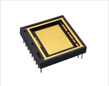
Ceramic Package
It is material made of the mineral such as alumina or zirconia sintered under high temperatures. It is used as the casing for the sensor, the high frequency part, the high power LED, the medical electronic part and the military electronic part. Since it is highly wear resistant, heat resistant, EMF shielding and corrosion resistant, it is used in highly reliable electronic parts.
Ceramic Package Features and Advantages
1. In general, it is used in applications required of high performance and reliability.
2. It is has high hardness and high modulus of elasticity, it is highly corrosion resistant and highly wear resistance and has a relatively low thermal expansion coefficient.
3. It has good high frequency properties, it is highly heat resistant and it is relatively easy to implement various temperature properties.
4. As it does not have polarity, it is favorable for board mounting.
5. It is increasingly used as set products such as mobile communication devices and digital home appliances which are digitalized, use higher frequency and become smaller.
Ceramic Material
Ceramic Material 
Alumina ALN Polyimide
(REF.)Si
(REF.)GaAs
(REF.)MDTB-900 MDTW-900 T.C.E.
[10-6/K]
6.7
R.T. -400C
6.8
R.T. -400C
4.4
R.T. -400C
20-70
R.T. -300C
3.6
R.T. -400C
6.0
R.T. -400C
Thermal Conductivity
[W/mk, R.T.]
17 17 170 0.2 125 54 Yung’s Modulus
[GPa]
280 280 350 3 - - Bending
Strength[MPa]
350 350 350 - 100 - ∂-Particle Count
[Count/cm2-h]
0.1 0.1 0.1 - - - Dielectric 1MHz R.T.
Constant 10GHz R.T.
9.4
8.89.8
9.08.9
8.53.2
-12.0
-13.1
-Dielectric 1MHz R.T.
Loss 10GHz R.T.
5×10⁻⁴
1×10-34×10-4
1×10-33×10-4
3×10-36×10-3
--
--
-Volume Resistivity
[Ωm]
1012 1012 1012 1012 108 10-8 - 10-6 Breakdown Voltage
[KV/mm]
15 15 15 300 - - - Applications
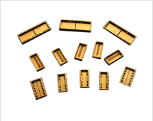
Applications (HTCC Application Product Case)
Applications (HTCC Application Product Case) Industry Usage Applied Product Package Crystal/Oscillator/SAW packages, Ceramic/Metal package, Hybrid packages,
Optical Package, Power dissipation package, Sensor packages, LED packages,
Monolithic microwave hybrid technologyIT and Electronics HTCC Amp housing, Custom pin grid array(PGA), High Frequency Feedthroughs,
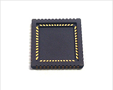
Leadless chip carriers(CLCC), Multichip module(MCM),
Pad array carriers(BGA), Quad Flat packs(QFP), Quad No lead(QFN)Optoelectronics CMOS, CCD, CLCC, Infrared, ultraviolet image sensor Resistance Curler, soldering iron, PTC, bidet and plasma reactor Vehicle Electric Part Power electronics PCB, LED lamp, honeycomb, PTC heater, ion generator, glow plug, etc. Semiconductor Equipment Probe Card, ESC, susceptor, boat, tube, chuck, etc. Bio Human Body Body material, artificial material and dental parts Related Images
-
Crystal / Oscillator / SAW PKG
-
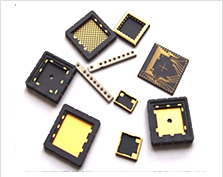
Sensor PKG
-
IR Sensor
-
RF PKG
-
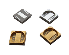
LED PKG
-
CLCC
Present and Future R&D Direction
Current R&D area is the insulating ceramic package which mainly uses HTCC (high temperature co-fired ceramic) and Al2O3 (alumina), of which internal electrode uses the metal with high melting point such as W, Mo or Mn for internal layer wiring and inter-layer conduction, and which is sintered at 1,500℃ or higher under reduction atmosphere with hydrogen, nitrogen or both, to meet required mechanical and electric characteristics.
As the semiconductor, mobile communication and LED markets have recently expanded significantly, the trend is wide growth of applications required of high temperature property, high chemical resistance, high thermal conductivity and mechanical strength, which LTCC (low temperature co-fired ceramic) cannot cover but HTCC can. In addition, as the mean to implement small sized, low cost and multi-functional ceramic electronic parts, HTCC is utilized in various areas including the board and the 3D component along with LTCC technology to complement each other.
Consequently, future R&D directions are development of the HTCC ceramic package for highly reliable electronic parts, and package development for highly added value industries including military electronics, IR sensor, aerospace housing and optoelectronic casing for communication, and multichip medical devices. To achieve it, the fundamental study should be accompanied with the basic ceramic property, the fine lamination technology, thermal property of the material, hybrid material joining technology and plating technology.
-
- Production Process
Ceramic Package production Process
Mixing and Milling
- Slurry Production Process
- The ceramic powder, the polymer bond, the dispersant and the solvent are evenly mixed.
- Well dispersed slurry is produced for moldability.
- Slurry Production Procedure
- Mixing Process: The mixer is used to produce physically and chemically uniform slurry.
- Dispersing Process: The dispersing equipment is used to apply the repulsive force to internal slurry particles to produce well dispersed slurry.
Tape Casting
- Forming Process
- The process of coating the uniform ceramic sheet on the forming PET film.
- Necessary Conditions for Uniform Ceramic Set Production
- Precise control technology on the formed article
- The best molding speed
- Constant drying condition
- Constant slurry feed speed
Clean Room Processing
- Printing
- The process of coating the internal electrode on the ceramic sheet.
- For the internal electrode pattern, the W-paste is coated on the ceramic sheet.
- Laminating
- The process of repeatedly layering each printed sheet as arranged.
- Cutting
- The process of cutting the laminated sheet in the bar state to the predefined size using the blade.
Sintering
- Process
- The thermal processing process to make the ceramic package with desired electric and mechanical characteristics.
- The formed article is sintered at 1600℃ or higher. The temperature and time profile should be carefully controlled.
- Step
- Step 1: Decomposition of the organic material used in the shaping work
- Step 2: Removal of hollow spaces, that is, pores between particles.
- Step 3: Densification and growing particles
Brazing (Metal Joining)
Technology metalizing the ceramic and joining it with the metal (Kovar and metallic alloy) by applying the filler metal and the heat (450°C or higher).
Plating
- Process
- The process to form the Ni-Au layer by electric and chemical reactions (electrolytic plating and non-electrolytic plating)
- Ni Plating: External electrode protection and joint
- Au Plating: Joint with the solder
- Target
- Enhanced solder weldability in the SMT process
- Electrode corrosion prevention
Batch & Milling
De-airing
Tape Casting
Tape Casting
Via Hole Punching
Patten Printing
Patten Printing
Cutting
Co-firing
Plating
Inspection
Packing